About us

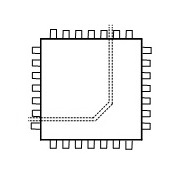
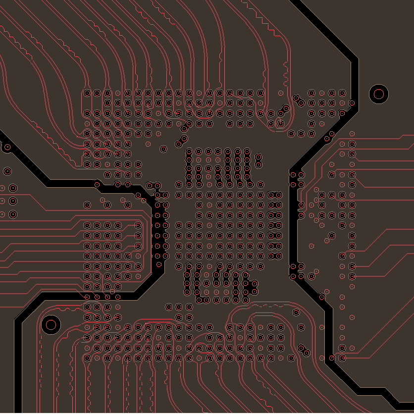
Otimal’s team of engineers contain expertise in high speed digital design, including, for example, SoCs and FPGAs, DDR3/DDR4, PCIe, SerDes. When it comes to designs with high speed digital, cross-talk potentially corrupting nearby signal nets. Each nearby net needs to be simulated as a ‘victim’ (i.e. FEXT & NEXT) of cross-talk using SI tools.
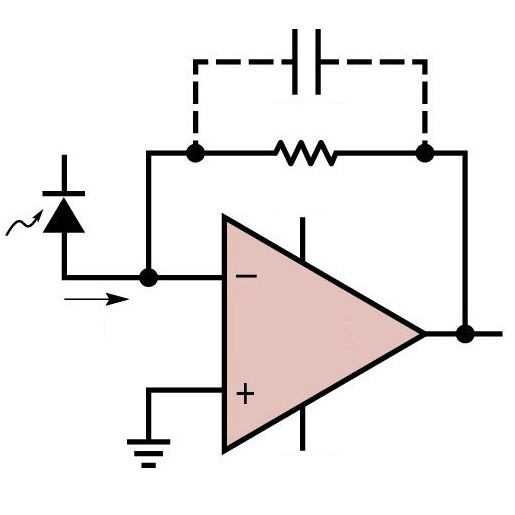
Certain analog designs can require a delicate touch in the design to ensure cleanly driven signals. Applications such as driving optical systems for LiDAR can require ultra-low ripple current or voltage drives which requires the expertise of Otimals engineers. Analog circuitry can be very sensitive to inductive or capacitive parasitics. Proper tuning procedures are utilized in order to make sure these effects are minimized
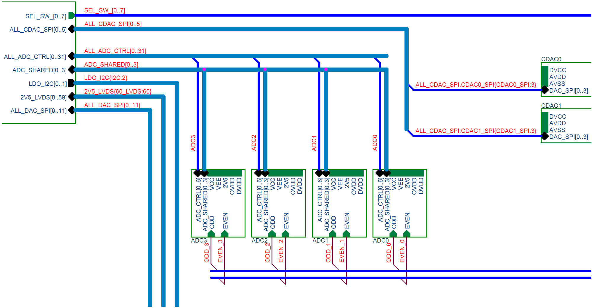
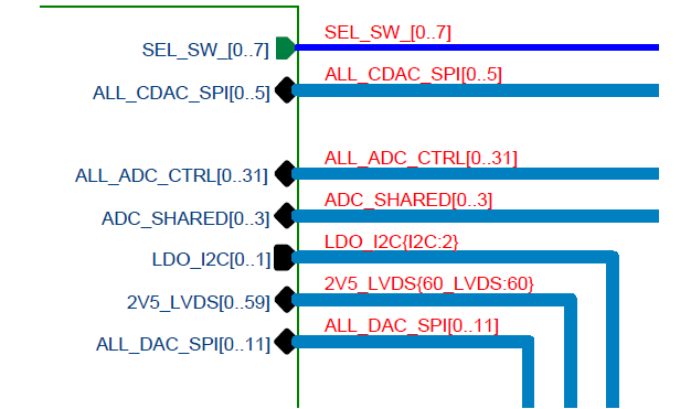
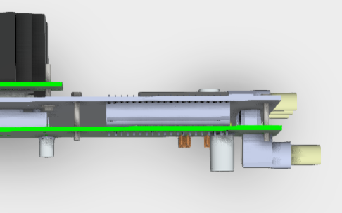
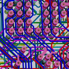
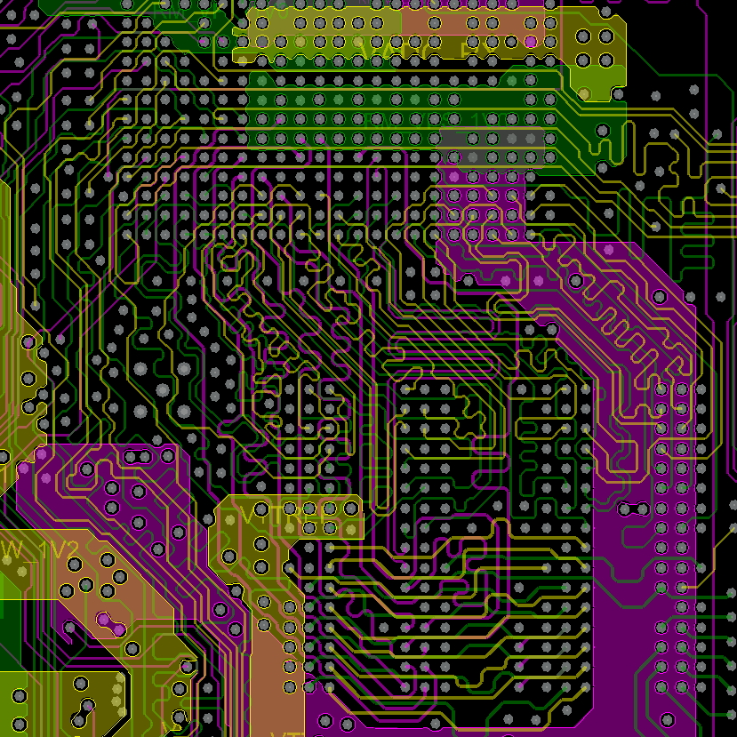
Otimal can design very complicated mixed-signal boards with many fine-pitch BGA FPGAs, PLLs, DDR, high-speed ADCs, Sensitive Analog Circuits, high-linearity chirp waveforms, etc. Various simulation and analysis tools are used to make sure that the cross-talk from the transients of the digital signals don’t interfere with the rest of the analog circuitry.

Here at Optimal, rigorous circuit simulations and analysis are done before doing the layout to ensure that the circuitry will operate and function as intended. The boards will be laid out with precise impedance control, which will be calculated and verified by the fabrication house chosen for the specific design. The RF transmission lines are careful routed and simulated to ensure proper isolation and to minimize return loss to maintain an optimal design. Custom stack-ups and exotic dielectrics can be used in the designs to meet your needs.
Otimal utilizes the right practices for high voltage designs by choosing the right materials and utilizing the best design practices. Boards can be designed well into the 100’s of kV, given the right choice of materials, such as HVPF (High Voltage Polyimide Film), a special dielectric material that can support up to 3kV/mil. Proper design guidelines are followed to decrease effects such as arcing and corona. Proper manufacturing steps are also taken to ensure good high voltage longevity and reliability, such as 260°F bake-outs and choosing the right dielectrics and prepregs for inner layers to avoid a void free press package.
Otimal follows strict guidelines for high current PCB design, aided by industry standards such as IPC-2152 “Standard for Determining Current-carrying Capacity in Printed Board Design.” Thermal conductivity, via current density, power dissipation, PCB material and thickness, and usage of copper planes are all elements of the design that are simulated and analyzed for thermal performance during the design phase before the board is sent out for fabrication.
An HDI PCB is a high-density interconnect PCB that has a very high signal net density, much smaller than normal trace/space pitch (i.e. 2-4mil). Laser drilled micro-vias (i.e. blind, buried, stacked), vias-in-pads, is generally used. A well designed HDI PCB can reduce layer count significantly while achieving better functionality.
HDI designs can also quickly become very expensive if the cost of the fabrication and assembly isn’t regularly updated and checked with board and assembly houses. Otimal also follows industry design guidelines and standards such as IPC-2315, IPC-2226, IPC-4104, and IPC-6016 for HDI PCB Design. This is why Otimal is the go-to PCB design firm for complicated HDI designs.
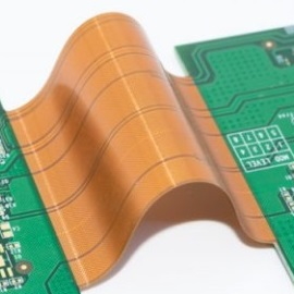
If any interconnect between PCBs or connectors need to find way through an unusual space, Otimal can design flex or rigid-flex PCBs to get the job done. The flex designs are done with important design rules in mind which ensure a long-term reliability of the flex boards and reduce possibilities of single-point failures. These design rules include designing the right stack-up while knowing your bend radius and layer count, choosing the proper (i.e. polyamide) dielectric material, using curved traces wherever possible, placing flex layers in the center of stack-ups, making via annular rings as large as possible, and adding teardrops to all connections and vias.
Every design done at Otimal is done with the intention of mitigating any sources of EMI. Placing bypass capacitors close to I/O and ground pins to avoid ground loops, utilizing solid ground planes, using ferrite beads wherever possible for clean power supply and grounding, keeping traces short, and avoiding unintentional antennas are all techniques used at Otimal among many others to ensure that the design functions as intended. Many of these techniques can even be simulated using various simulation tools, such as bypass capacitor values/quantity, EMI scans, etc.

Otimal’s full turnkey design process includes designing for manufacturability, assembly, and test. This makes sure that the PCB will meet the client’s specifications and functional requirements while maintaining an optimal yield and reliability factor.

Otimal works with PCB fabrication and assembly houses to ensure that the designs are done properly for manufacturability and assembly. Otimal also provides a database including the design schematics and PCB libraries, BOM, critical datasheets, project design files, assembly drawings, fabrication drawings, and test instructions.
FPGA, DDR3, High-Speed digital
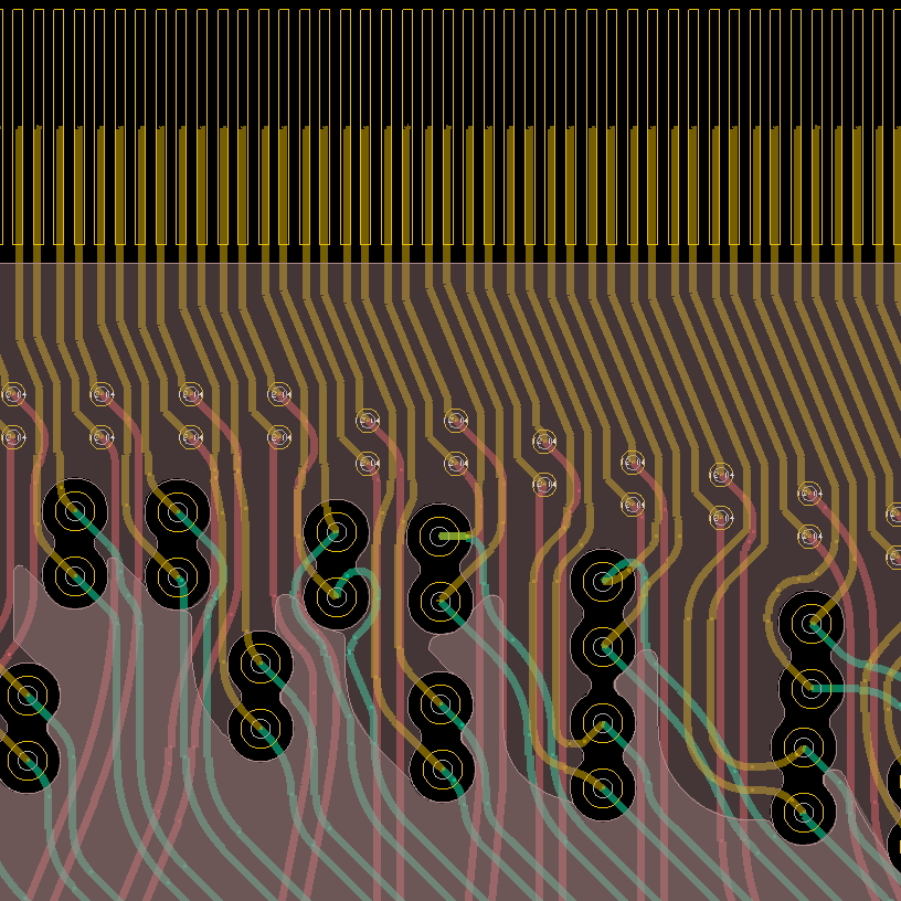
HDI, lazer via
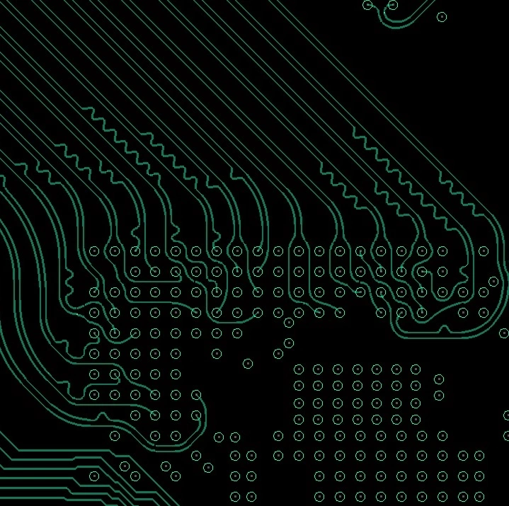
Differential signal, length matching
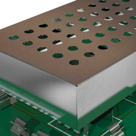
Mixed-signal board
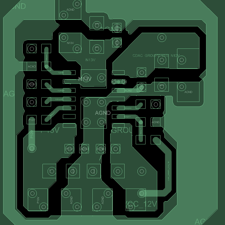
Low-noise power supply